Harmony Industry Diamond (H.I.D.)
Harmony Industry Diamond (H.I.D.)
The third generation semiconductor devices have excellent thermal and electrical conductivity, and have a wide application prospect in the field of high temperature, high frequency, high power and radiation resistance integrated electronic devices
Semiconductor is a substance with electrical conductivity between insulator and conductor. The difference between semiconductor and insulator mainly comes from the different band widths.
In the industry, the so-called "generation" division of semiconductors refers to the division by material:
[First generation semiconductor] mainly refers to the semiconductor devices with silicon (Si) and germanium (Ge) as materials.
[Second-generation semiconductor] refers to compound semiconductor mainly composed of gallium arsenide (GaAs) and indium antimonide (InSb).
[Third generation semiconductor] includes wide-band gap compound semiconductors represented by silicon carbide (SiC) and gallium nitride (GaN). Silicon carbide and gallium nitride have their own advantages and disadvantages in material properties, so they have different emphasis and complementarity in the application field.
Among the third-generation semiconductor materials, SiC has the characteristics of large forbidden band width, high breakdown electric field, high saturation electron drift speed, and large thermal conductivity, and can be applied to high-voltage environments above 1200 volts, so it has obvious advantages in harsh environments and can be widely used in modern industrial fields such as new energy vehicles, 5G communications, photovoltaic power generation, rail transportation, smart grid, and aerospace.
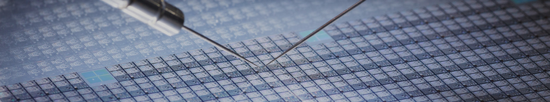
However, the high hardness, high brittleness, good wear resistance and extremely stable chemical properties of SiC crystals make the processing of SiC wafers very difficult. Diamond, on the other hand, is the hardest substance known to exist naturally and is best suited for processing SiC wafers.
The ultra-precision machining process of SiC single crystal wafers, according to its processing sequence, mainly goes through the following processes: multi-line cutting, double-sided rough grinding, double-sided fine grinding, double-sided chemical mechanical polishing and Si-side CMP.
Semiconductor is a substance with electrical conductivity between insulator and conductor. The difference between semiconductor and insulator mainly comes from the different band widths.
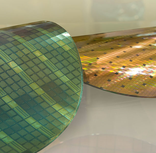
As a typical third-generation semiconductor material, gallium nitride (GaN) is difficult to prepare in wafer preparation technology. As the single crystal material for the preparation of gallium nitride cannot be directly obtained from nature, the main preparation method of gallium nitride is epitaxy on sapphire, silicon carbide, silicon and other heterogeneous substrates.
At present, two thirds of GaN devices are used in military electronics, such as military communications, electronics, jamming, radar and other fields. In the civil field, gallium nitride is mainly used in communication base stations, power devices and other fields. In the future, it will be widely used in 5G base stations, new energy vehicles, ultra-high voltage, data centers and other scenarios.
The ultra-precision processing of gallium nitride substrate mainly goes through the following processes according to its processing sequence: double-sided grinding, single-side fine grinding and single-side fine polishing.