Harmony Industry Diamond (H.I.D.)
Harmony Industry Diamond (H.I.D.)
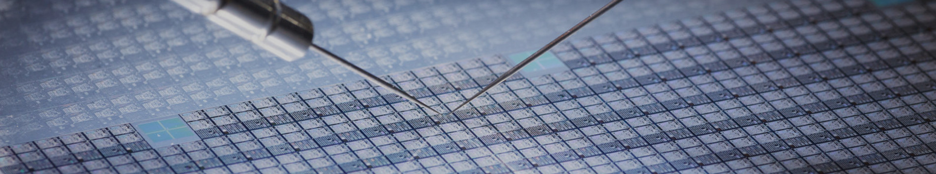
In semiconductor packaging, a ceramic substrate is a special process plate in which copper foil is bonded to the surface of the ceramic substrate direcly (single or double-sided) at high temperature. The mainly types include Beryllium Oxide (BeO), Alumina (Al2O3) and Aluminum Nitride (AlN), Silicon Nitride (Si3N4).
In semiconductor packaging, a ceramic substrate is a special process plate in which copper foil is bonded to the surface of the ceramic substrate direcly (single or double-sided) at high temperature. The mainly types include Beryllium Oxide (BeO), Alumina (Al2O3) and Aluminum Nitride (AlN), Silicon Nitride (Si3N4).
In semiconductor packaging, a ceramic substrate is a special process plate in which copper foil is bonded to the surface of the ceramic substrate direcly (single or double-sided) at high temperature. The mainly types include Beryllium Oxide (BeO), Alumina (Al2O3) and Aluminum Nitride (AlN), Silicon Nitride (Si3N4).

1. Strong mechanical stress and stable shape;
2. Excellent thermal cycle performance, cycle times up to 550,000, high reliability;
3. Same with PCB board ((or IMS substrate)) can be etched out of a variety of graphic structure;
4. No pollution and pollution-free;
5. Wide temperature range -55℃~850℃;
6. Thermal expansion coefficient is close to silicon, simplifying the production process of power module.